

 English
 français
 Deutsch
 español
 العربية
 中文
中文
Prehistoric era -PT
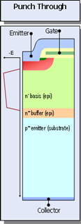
PT is the earliest generation of IGBT. It uses heavily doped P+substrate as the starting layer, on which N+buffer and N-base epitaxy are successively grown, and finally the cellular structure is formed on the surface of the epitaxy layer. It is named because the electric field runs through the entire N-base region at the cut-off time. Its process is complex, its cost is high, and it needs carrier life control. The saturation voltage drop is negative temperature coefficient, which is not conducive to parallel connection. Although it was a storm in the 1980s, it was gradually replaced by NPT in the late 1980s. At present, it has been hidden in the world. At present, all IGBT products of Infineon do not use PT technology.
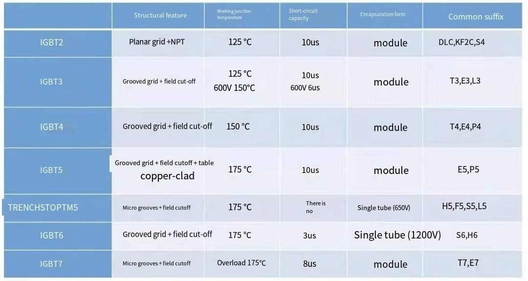
Early Leader - IGBT2
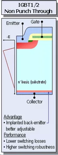
Features: planar gate, non-penetrating structure (NPT)
NPT-IGBT emerged in 1987 and soon became the hegemon in the 1990s. The difference between NPT and PT is that it uses the low-doped N-substrate as the starting layer, first makes MOS structure on the front of the N-drift region, then uses the grinding thinning process to reduce the thickness from the back to the thickness required by the IGBT voltage specification, and then uses the ion implantation process to form a P+collector from the back. At the cut-off time, the electric field does not penetrate the N-drift region, so it is called "non-penetrating" type IGBT. NPT does not need carrier lifetime control, but its disadvantage is that if higher voltage blocking capability is required, it will inevitably require a higher resistivity and thicker N-drift layer, which means that the saturated on-voltage Vce (sat) will also rise, thus greatly increasing the loss and temperature rise of the device.
Skills: low saturation pressure drop, positive temperature coefficient, 125 ℃ working junction temperature, high robustness
Positive temperature coefficient, convenient for parallel connection.
Name: DLC, KF2C, S4
Wait, it seems that something strange is mixed in!
No mistake! S4 is really not IGBT4, it is IGBT2 with red roots. It is suitable for high-frequency switching applications. The hard switching frequency can reach 40kHz. This star product still sells well.
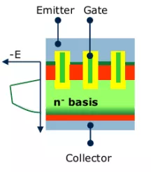
Performance leap-IGBT3
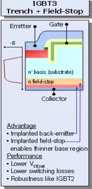
Features: trench gate, field stop
The emergence of IGBT3 has set off a huge revolution in the field of IGBT. The cell structure of IGBT3 has changed from plane type to groove type. In grooved IGBT, the electronic channel is perpendicular to the surface of the silicon wafer, which eliminates the JFET structure, increases the density of the surface channel, and improves the near-surface carrier concentration, thus making the performance more optimized. (Refer to the article "Structural analysis of planar and grooved IGBT" for the difference between planar and grooved gate technology).
In terms of longitudinal structure, in order to alleviate the contradiction between blocking voltage and saturation voltage drop, Yingjia launched Field Stop IGBT in 2000, aiming to minimize the thickness of drift zone and thus reduce saturation voltage. The starting material of the field stop IGBT is the same as that of the NPT, both of which are low-doped N-substrates. The difference is that the back of the FS IGBT is injected with an additional N buffer layer, and its doping concentration is slightly higher than that of the N-substrate. Therefore, the intensity of the electric field can be rapidly reduced, making the overall electric field trapezoidal, thus greatly reducing the required thickness of the N-drift region. In addition, the N buffer can also reduce the emission efficiency of the P emitter, thus reducing the trailing current and loss when turning off. (For more information about the difference between NPT and field cut-off devices, please refer to the difference between PT, NPT and FS IGBT).
Skills: low conduction voltage drop, 125 ℃ working junction temperature (150 ℃ for 600V devices), switch performance optimization
Due to the field cutoff and grooved cell, the on-state voltage drop of IGBT3 is lower, and the typical Vce (sat) ranges from 3.4 in the second generation to 2.55V in the third generation (3300V for example).
Name: T3, E3, L3
IGBT3 has been basically replaced by IGBT4 in the medium and low voltage field, but it still dominates in the high voltage field. For example, the mainstream products of 3300V, 4500V and 6500V still use IGBT3 technology.
The mainstay - IGBT4
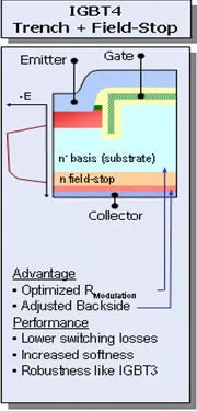
IGBT4 is the most widely used IGBT chip technology at present. The voltage includes 600V, 1200V, 1700V, and the current ranges from 10A to 3600A. It can be seen in various applications.
Features: trench gate+field cut-off+thin wafer
Like IGBT3, it is a field cut-off+groove gate structure, but IGBT4 optimizes the back structure, the thickness of the drift zone is thinner, and the doping concentration and emission efficiency of the back P emitter and N buffer are optimized.
Skills: high switching frequency, optimized switching softness, 150 ℃ working junction temperature
IGBT4 further reduces the switching loss by using thin wafers and optimizing the back structure, while the switching softness is higher. At the same time, the maximum allowable operating junction temperature has increased from 125 ℃ in the third generation to 150 ℃, which will undoubtedly further increase the output current capacity of the device.
Name: T4, E4, P4
T4 is a low-power series with a maximum switching frequency of 20kHz.
E4 is suitable for medium power applications, with a maximum switching frequency of 8kHz.
P4 further optimizes the switching softness, which is more suitable for high-power applications, and the switching frequency is up to 3kHz.
Rich man comes on stage - IGBT5
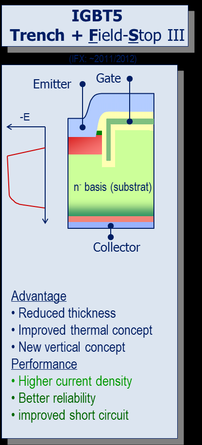
Features: trench gate+field cut-off+surface covered with copper
IGBT5 is the most luxurious product in all IGBT series. Other chips use aluminum for surface metallization. IGBT5 uses thick copper instead of aluminum. Copper's current capacity and heat capacity are far better than aluminum, so IGBT5 allows higher working junction temperature and output current. At the same time, the chip structure is optimized, and the chip thickness is further reduced.
Skills: 175 ℃ working junction temperature, 1.5V saturation voltage, output current capacity increased by 30%
Because the surface of IGBT5 is coated with copper and the advanced. XT packaging technology is adopted in the module packaging, the working junction temperature can reach 175 ℃. Compared with IGBT4, the chip thickness is further reduced, making the saturation voltage drop lower and the output current capacity increased by 30%.
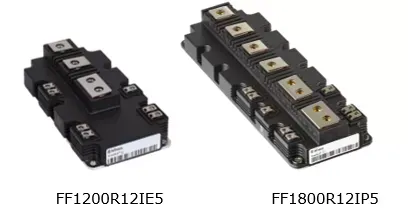
Name: E5, P5
At present, IGBT5 chips are only packaged in PrimePACK ™ In addition, the voltage is only 1200V and 1700V, representing products FF1200R12IE5 and FF1800R12IP5.
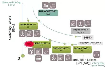
True and False Monkey King - TRENCHSTOP ™ 5
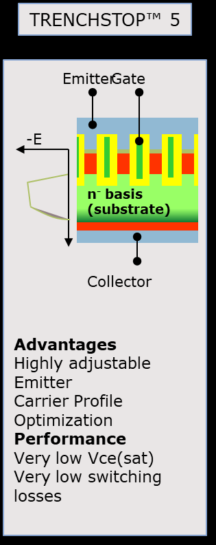
In the single management sector, there is a category of products called TRENCHSTOP ™ 5。 I often hear people ask if H5, F5, S5 and L5 are IGBT5? Strictly speaking, it is not. Although the name has 5 in it, H5, F5 and S5 belong to another family called TRENCHSTOP ™ 5。 This family has no "golden armor" blessing, and the gene is also different from IGBT5.
Features: fine groove grid+field cutoff
Although they are all called trench grids, TRENCHSTOP ™ They are still very different from their predecessors. It has more dense channels and higher current density. It does not have short circuit capability while achieving the best operating performance.
Skills: 175 ℃ maximum working junction temperature, high switching frequency, no short circuit capability
Performance and short circuit are always a contradiction. In order to pursue excellent performance, TRENCHSTOP ™ 5 Short circuit time is sacrificed. TRENCHSTOP ™ 5 According to different application purposes, extremely low conduction loss or extremely high switching frequency can be achieved, with the maximum switching frequency of 70~100kHz, and the minimum conduction voltage drop can be as low as 1.05V.
Name: H5, F5, S5, L5
TRENCHSTOP ™ At present, there are only 650V devices, and they are all discrete devices. This series of products optimize the on-state loss and switching loss for different applications. H5/F5 is suitable for high-frequency applications, and L5 has the lowest conduction loss. TRENCHSTOP ™ 5 The position of each product on the compromise curve is shown in the figure below.
Rising star - IGBT6
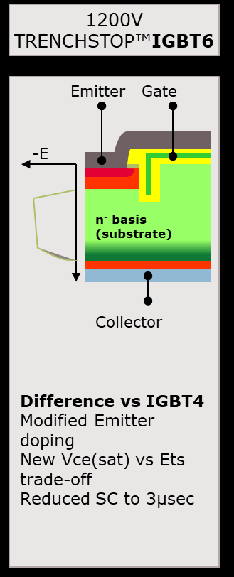
Although there is a gap of 5 between the 6th generation and the 4th generation, the 6th generation is actually the optimized version of the 4th generation, which is still the trench gate+field cutoff. IGBT6 is currently only used in single tube.
Features: trench grid+field cutoff
The device structure is similar to that of IGBT4, but the back P+injection is optimized to obtain a new compromise curve.
Skill: 175 ℃ maximum working junction temperature, Rg controllable, 3us short circuit
IGBT6 currently has two series of products, S6 has low conduction loss, Vce (sat) 1.85V; H6 has low switching loss, which is 15% lower than H3.
Name: S6, H6
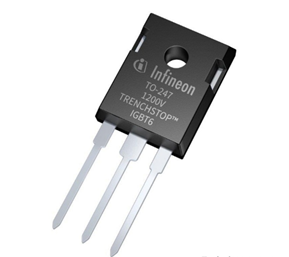
IGBT6 only has single-tube packaging products, such as IKW15N12BH6, IKW40N120CS6, which are packaged with TO-247 3Pin, TO-247 plus 3Pin, and TO-247 plus 4pin.
Great attention - IGBT7
After several generations of accumulation, IGBT finally ushered in IGBT7 in 2018.
Features: micro-groove gate+field cutoff
Although they are all grooved grids, the whole structure will be very different if there is one more microword. The IGBT7 channel density is higher, the cell spacing is also carefully designed, and the parasitic capacitance parameters are optimized to achieve the best switching performance at 5kv/us.
Skill: 175 ℃ overload junction temperature, dv/dt controllable
Compared with IGBT4, IGBT7 Vce (sat) is reduced by 20%, which can achieve a maximum transient operating junction temperature of 175 ℃.
Name: T7, E7
Representative products include: FP25R12W1T7. T7 is optimized for motor driver, which can achieve the best performance at 5kv/us. E7 is more widely used, including electric commercial vehicle driver, photovoltaic inverter, etc.
YTPQC-AHF、SVG
YTPQC-AHF(Active harmonic filter)、SVG (Static Var Generator) mainly use 5th insulated gate bipolar transistor (IGBT) to control the magnitude and phase of inverter AC voltage, so as to achieve the purpose of harmonic filtering , reactive power compensation and 3 phase load balancing .
In terms of reliability, due to the lack of popularity, the reliability of the higher generation IGBT is lower than that of the lower generation IGBT.
The seventh generation IGBT has higher frequency and faster speed. Which will lead to smaller volume of other components used by it, so the overall volume of the module is smaller. For our industry, the main difference is product volume. In terms of product volume, we are currently developing a new 2U module, which has a considerable compensation capacity with a smaller volume


 IPv6 network supported